Characterization of 4H-SiC MOSFETs
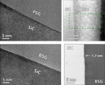
This project was part of my Ph.D. research while at the University of Maryland. It focused on analyzing the impacts of various fabrication processes on 4H-SiC wide bandgap MOSFET devices. Specifically, we were interested in the passivation of electrically active atomic-scale defects at the interface between SiC and SiO$_\sf{2}$. To analyze these defects, we used a combination of high resolution and scanning transmission electron microscopy (HRTEM and STEM), together with analytical TEM using electron energy loss spectroscopy (EELS).
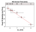
Through the course of this project, we revealed that nitric oxide (NO) device annealing results in a narrowing of the atomic-scale transition layer that exists between SiC and SiO$_\sf{2}$ as the concentration of nitrogen increases. We further discovered using X-ray photoelectron spectroscopy (XPS) that the bonding state for Si atoms within the transition layer changes slightly upon NO annealing. Using advanced multivariate analysis techniques, we were able to probe the nature of these interfacial states using EELS. NO annealing was found to cause changes in the bonding of Si, C, and O at the interface, attributable to the presence of interfacial nitrogen. Finally, we investigated the impacts of boron- and phosphorus-based passivation strategies to see how their effects varied compared to NO. Both of these newer processing approaches had significantly higher influence on the structure of the oxide than NO, explaining the origins of some instabilities observed in their corresponding MOSFET devices.
This project was highly collaborative in nature, involving researchers from the U.S. Army Research Laboratory, Auburn University, and Rutgers University.
Some highlights of the project:
- Used high resolution TEM and electron energy loss spectroscopy to investigate the effects of post-processing on SiC MOSFETs
- Implemented novel EELS methodologies to probe the nature of the interfacial transition layer in SiC MOS devices
- Discovered unique electronic states of silicon in nitric oxide annealed devices using unsupervised machine learning EELS analyses
- Developed oxide spin-etching process with monolayer sensitivity for XPS depth profiling
Publications
Analysis of the electronic and chemical structure in boron and phosphorus passivated 4H-SiC/SiO$_\sf{2}$ interfaces using HRTEM and STEM-EELS
Advanced Analytical Microscopy at the Nanoscale: Applications in Wide Bandgap and Solid Oxide Fuel Cell Materials
Systematic structural and chemical characterization of the transition layer at the interface of NO-annealed 4H-SiC/SiO$\sf_2$ metal-oxide-semiconductor field-effect transistors